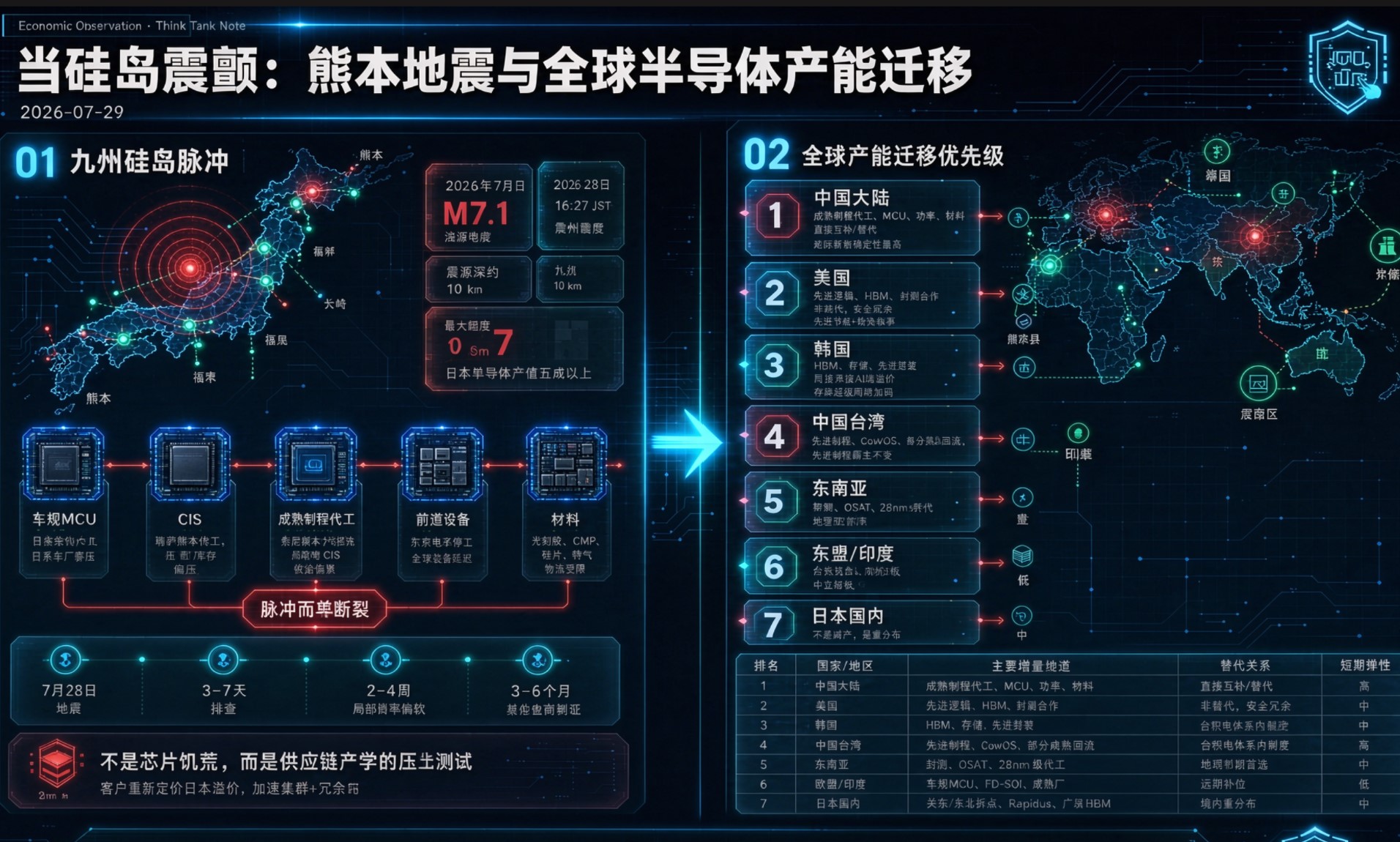
When the Silicon Island Shakes: Kumamoto Quake and the Global Semiconductor Supply Chain
当"硅岛"震颤:熊本地震与世界半导体供应链的观察札记
Economic Observation · Think Tank Note / 经济观察·智库札记
2026-07-29
Ⅰ. The Epicenter Was Not Just under Kumamoto — It Was under the Supply Chain
一、震中不仅在熊本地下,也在供应链的软腹上
At 16:27 JST on 28 July 2026, a M7.1 shallow quake (depth ~10 km, max seismic intensity 7) struck Kumamoto Prefecture. The headline number is geological; the real story is industrial. Kumamoto sits inside Kyushu — "Silicon Island" — where over half of Japan's semiconductor output value is generated, spanning foundry, CIS, automotive MCU, power devices, front-end equipment, photoresist, CMP slurries, silicon wafers and packaging materials.
2026年7月28日16:27(日本时间),熊本县发生7.1级浅源地震(震源深约10公里,最大震度7)。地质数字只是引子,产业才是正文。熊本嵌在九州"硅岛"之中——这里贡献日本全国半导体产值五成以上,覆盖晶圆代工、CIS、车规MCU、功率器件、前道设备、光刻胶、抛光液、硅片与封装材料全链条。
Unlike 2016, when structures cracked, this round of shutdowns is precautionary, not destructive:
与2016年熊本地震不同,本轮停产以预防性停机为主,而非厂房崩裂:
-
JASM (TSMC Japan) Kumamoto Fab-1 (28/22/16/12 nm, ~20k wafers/month, ~2.6% of TSMC capacity): staff evacuated, building cleared, gradually re-entering line; Fab-2 construction paused for aftershock safety.
-
Sony Semiconductor Kikuyo / Koshi CIS plants: reinforced structures intact, tech center still under inspection, other Kyushu bases (Nagasaki/Oita/Kagoshima) unaffected.
-
Renesas Kawajiri & Nishiki MCU fabs: ceiling panels dropped, wall cracks, pure-water pause; cleanroom utilities maintained, tool recalibration pending.
-
Tokyo Electron Koshi & Otsu equipment fabs: no major damage, full-day halt on 29 July for safety audit (coater/developer, cleaner, 3D-packaging kit).
-
Mitsubishi Electric power/SiC, Fuji Film materials, Toppan packaging, Tokai Carbon, Horiba, Ebara parts — all in stop-and-check mode.
The physical damage is minor; the micro-displacement of precision tools is the real clock. A 0.1-micron shift in a litho or coater tool can force 3–7 days of recalibration; pessimistic cases run 2–4 weeks before yield stabilizes.
物理损毁很小,精密机台的微米级位移才是真正的计时器。光刻或涂胶设备偏移0.1微米即需3–7天重校准;悲观情形下良率回稳要2–4周。
Ⅱ. Five Pressure Points on the World Map
二、打在世界地图上的五个压力点
The quake did not hit "semiconductors" uniformly. It hit five nodes where Kyushu holds disproportionate weight:
地震不是均匀砸向"半导体",而是精准砸在九州权重异常的五个节点:
1. Automotive MCU / 车规MCU
Renesas Kumamoto is a global anchor for automotive microcontrollers. With Toyota/Honda/Mazda lean-inventory lines, the 2016 precedent suggests a 2–4 week lag before a fab pause becomes a vehicle-line pause.
瑞萨熊本是车规MCU全球锚点。日系车企按精益库存排产,2016年经验是工厂停摆2–4周后传导到整车端。
2. CMOS Image Sensors / 车载与手机CIS
Sony's Kumamoto cluster feeds smartphone main cameras and ADAS lenses. No structural damage, but any tool downtime trims near-term high-end CIS supply exactly when automotive camera count per car is rising (L2+ needs 8–12 modules).
索尼熊本集群供养手机主摄与ADAS镜头。厂房无损,但机台停机恰逢单车摄像头数量上行(L2+需8–12颗),短期高端CIS供给被削角。
3. Mature-node foundry (12–28 nm) / 成熟制程代工
JASM Fab-1 is a regional breadbasket for Japan's auto & industrial clients, not a global advanced-node pillar. Its ~2.6% share of TSMC means no worldwide crunch, but Japanese and some European auto tiers feel the pinch harder than Taiwan or Korea.
JASM一厂是日本汽车与工业客户的区域粮仓,不是全球先进制程支柱。占台积电总产能约2.6%意味着无全球断供,但日本及部分欧洲车系比台湾、韩国更疼。
4. Front-end equipment & parts / 前道设备与零配件
Tokyo Electron's Kumamoto sites ship coater/developers and 3D-packaging tools; Ebara/Horiba supply vacuum & flow-control parts. Equipment lead times are already long (12–18 months); a 1-week inspection stall delays global tool installations, not just local wafers.
东京电子熊本出厂涂胶显影与3D封装设备,荏原/堀场供真空与流量零配件。设备交期本就12–18个月,停工1周拖延的是全球机台装机,不止本地晶圆。
5. Materials: photoresist, CMP, wafer, specialty gas / 材料:光刻胶、抛光、硅片、特气
Kyushu hosts TOK, JSR, Shin-Etsu, Fujifilm, Taiyo Nippon Sanso adjacencies. Even a logistics pause (rail/power/trucking) in Kumamoto compresses just-in-time delivery of high-purity chemicals where buffer stock is deliberately thin.
九州周边聚拢东京应化、JSR、信越、富士胶片、大阳日酸。即便只是物流暂停(铁路/电力/卡车),也会压缩高纯化学品的准时交付——这类物料行业故意不留厚库存。
Ⅲ. Why This Is a "Pulse," Not a "Break"
三、为什么这是脉冲,不是断裂
Three structural facts cap the damage:
三个结构性事实把破坏上限锁住了:
-
Seismic-grade fabs: Post-1995 Kobe and 2016 Kumamoto retrofits mean Japanese semiconductor buildings tolerate intensity 7; the vulnerability is tools, not roofs.
抗震级厂房:1995阪神、2016熊本后 retrofit 标准下,日本半导体建筑抗7级,弱点在机台不在屋顶。
-
Redundant geography: Sony has Nagasaki/Oita/Kagoshima; Renesas has Naka/Hitachi; TSMC can lean on Taiwan/Korea/GlobalFoundries for mature node; Shin-Etsu has Gunma/Yamanashi. No single point is irreplaceable.
地理冗余:索尼有长崎/大分/鹿儿岛,瑞萨有那珂/日立,台积电可回台湾/韩国补成熟制程,信越有群马/山梨。没有单点不可替代。
-
Inventory buffers post-2020–2022 crisis: OEMs and automakers learned from the COVID chip famine; safety stock for MCU/CIS is weeks, not days.
2020–2022缺芯后的缓冲:车厂与OEM学过饥荒课,MCU/CIS安全库存按周计,不是按天计。
Thus the base case: 3–7 days inspection, 2–4 weeks partial yield softness, no multi-quarter global shortage. Spot prices for automotive MCU and certain CIS may tick up; sustained re-pricing is unlikely unless a magnitude-7 aftershock hits within 72 hours.
所以基准情景:3–7天排查,2–4周局部良率偏软,无跨季度全球紧缺。车规MCU与部分CIS现货价可能小翘,但除非72小时内再来一次7级余震,否则难成趋势性涨价。

Ⅳ. The Real Output: Supply-Chain Philosophy, Not Chip Count
四、真正产出:供应链哲学,而非芯片数量
The quake's lasting effect is less about wafers and more about governance narrative:
地震的长尾不在晶圆数,而在治理叙事:
-
"Cluster + redundancy" beats "cluster only." Kyushu's density gave Japan scale; the quake re-proves that extreme regional concentration trades efficiency for resilience. Expect more second-source qualification for automotive MCU, CIS, photoresist and coater tools.
"集群+冗余"胜过"纯集群"。九州密度给了日本规模,地震再证极端区域集中是用韧性换效率。车规MCU、CIS、光刻胶、涂胶设备将加速第二供应商认证。
-
Geopolitics and geology converge. US/EU/Japan industrial policy already pushes "friend-shoring"; a quake on a fault line is a non-political reminder that natural risk is also strategic risk.
地缘与地质合流。友岸外包本就是政策题,断层带上的地震提醒:自然风险也是战略风险。
-
Buyers re-price "Japan premium." Japanese materials/equipment carry quality premium; now buyers internalize a seismic insurance cost into sourcing math — not by leaving Japan, but by keeping dual lanes warm.
重估"日本溢价"。日系材料设备有质量溢价,现在采购方会把地震保险费算进选型——不是离开日本,而是保留双车道热备。
Ⅴ. Global Ripple, Not Global Shortage
五、全球涟漪,非全球断供
-
Automotive: Japanese OEMs first; European second-tier EV makers with Renesas-heavy BOMs third; Chinese NEV supply chains largely decoupled from Kumamoto MCU/CIS loop → limited direct hit.
汽车:日系最先,欧系二线EV次之,中国新能源链与熊本MCU/CIS解耦度高→直接命中有限。
-
Smartphone / consumer: CIS high-end tightness possible in Q3 2026; mid-low CIS unaffected.
消费电子:2026 Q3高端CIS可能紧,中低端无碍。
-
Industrial & IoT: mature-node (12–28 nm) lead time may extend 1–2 weeks for Japan-bound orders; global pool absorbable.
工业IoT:去日本方向的12–28nm交期或延1–2周,全球池子可吸。
-
Equipment install base: TEL/Ebara/Horiba recalibration stalls global tool commissioning 1–2 weeks; capex timelines slip, not cancel.
设备存量:TEL/荏原/堀场校准拖慢全球装机1–2周,资本开支时间表滑移不取消。
Kumamoto 2026 is not the "chip famine" of 2021. It is a stress test broadcast in real time — proving that the world's semiconductor system can absorb a M7.1 on the Silicon Island, but cannot pretend the Island is insulated from the earth. Resilience, not relocation, is the lesson. The fabs will restart; the sourcing maps will quietly redraw.
2026熊本不是2021缺芯饥荒。它是一场实时播出的压力测试——证明世界半导体系统扛得住硅岛7.1级震动,却不能再假装硅岛与大地无关。教训是韧性,不是搬迁。厂房会重启,采购地图会静默重绘。
— Observation desk, 2026-07-29
此文由 怡心湖 编辑,若您觉得有益,欢迎分享转发!:首页 > 观·世界 » 当"硅岛"震颤:熊本地震与世界半导体供应链的观察札记
 从两极到战国:双线热战背景下的全球
 斗牛士的“长期主义”:为何西班牙足
 世界公民:理想主义的引力与民族国家