极寒之舞与原子之雨:超导铌材与高性能钽靶坯的微观世界征途
Dance in the Cold, Rain of Atoms: The Microscopic Odyssey of Superconducting Niobium and High-Purity Tantalum Sputtering Targets
在人类探索物质边界的征途中,有两种看似不起眼的银灰色金属,正悄然支撑着现代科技的脊梁。它们不似黄金般耀眼,也不像稀土那样常被舆论提及,但它们却分别掌管着“极寒下的零损耗输电”与“芯片上的原子级雕刻”。这便是铌(Niobium)与钽(Tantalum)。
In humanity's quest to push the boundaries of matter, two unassuming silvery-gray metals quietly uphold the backbone of modern technology. They lack the luster of gold or the media spotlight often enjoyed by rare earths. Yet, they govern "zero-loss power transmission in extreme cold" and "atomic-scale sculpting on microchips," respectively. These are Niobium and Tantalum.
本文将带你深入微观世界,探寻超导铌材如何在接近绝对零度的环境中翩翩起舞,以及高性能钽靶坯如何在半导体制造中降下一场精准的“原子之雨”。
This article delves into the microscopic realm to explore how superconducting niobium dances in environments near absolute zero, and how high-performance tantalum sputtering targets unleash a precise "rain of atoms" in semiconductor fabrication.
第一章:极寒之舞——超导铌材的物理诗篇
Chapter 1: Dance in the Cold — The Physical Poetry of Superconducting Niobium
1.1 从迈斯纳效应说起
1.1 Starting with the Meissner Effect
超导现象,是量子物理赐予宏观世界的奇迹。当温度降低至临界值以下,某些材料的电阻会瞬间消失,同时表现出完全抗磁性——即迈斯纳效应(Meissner Effect)。这意味着磁场线无法穿透超导体,超导体仿佛穿上了一层“隐形的盔甲”,将磁力线完全排斥在外。
Superconductivity is a miracle granted by quantum physics to the macroscopic world. When the temperature drops below a critical threshold, the electrical resistance of certain materials vanishes instantaneously. Concurrently, they exhibit perfect diamagnetism—the Meissner Effect. This implies that magnetic field lines cannot penetrate the superconductor; it dons an "invisible armor," completely expelling magnetic flux.
在所有超导材料中,金属铌以其独特的优势脱颖而出。它是目前已知在最高临界温度(约9.2K)下工作的单质超导体之一。更重要的是,铌在超导状态下的射频(RF)性能极佳,能够承载极高的加速电场而不产生热量损耗。这使得它成为了粒子加速器领域的“无冕之王”。
Among all superconducting materials, niobium stands out due to its unique advantages. It is one of the elemental superconductors known to operate at the highest critical temperature (approx. 9.2K). More importantly, niobium exhibits exceptional radio-frequency (RF) performance in its superconducting state, capable of sustaining extremely high accelerating fields without thermal losses. This has crowned it the "uncrowned king" of the particle accelerator domain.
1.2 铌射频超导腔:捕捉闪电的瓶子
1.2 Niobium RF Cavities: Bottles That Capture Lightning
如果说普通的电线是电流的公路,那么铌射频超导腔(Niobium RF Superconducting Cavity)就是粒子加速器的“心脏起搏器”。
If ordinary wires are highways for electric current, then the niobium RF superconducting cavity is the "pacemaker" for particle accelerators.
这些腔体通常由高纯铌材冲压焊接而成,形状如同巨大的保温瓶内胆或复杂的几何雕塑。当液氦将其冷却至2K(零下271摄氏度)左右的极低温时,铌材进入超导态。此时,注入腔体的微波能量不再被腔壁吸收转化为热量,而是近乎无损地在腔内振荡。这种振荡产生的强大电场,能将电子或质子加速到接近光速。
These cavities are typically fabricated from high-purity niobium via stamping and welding, resembling giant thermos flasks or intricate geometric sculptures. When cooled to around 2K (minus 271 degrees Celsius) using liquid helium, the niobium enters its superconducting state. At this point, microwave energy injected into the cavity is no longer absorbed and converted into heat by the walls; instead, it oscillates within the cavity with negligible loss. The powerful electric fields generated by this oscillation accelerate electrons or protons to velocities approaching the speed of light.
技术难点在于“纯度”与“洁净”。
The technical hurdles lie in "Purity" and "Cleanliness."
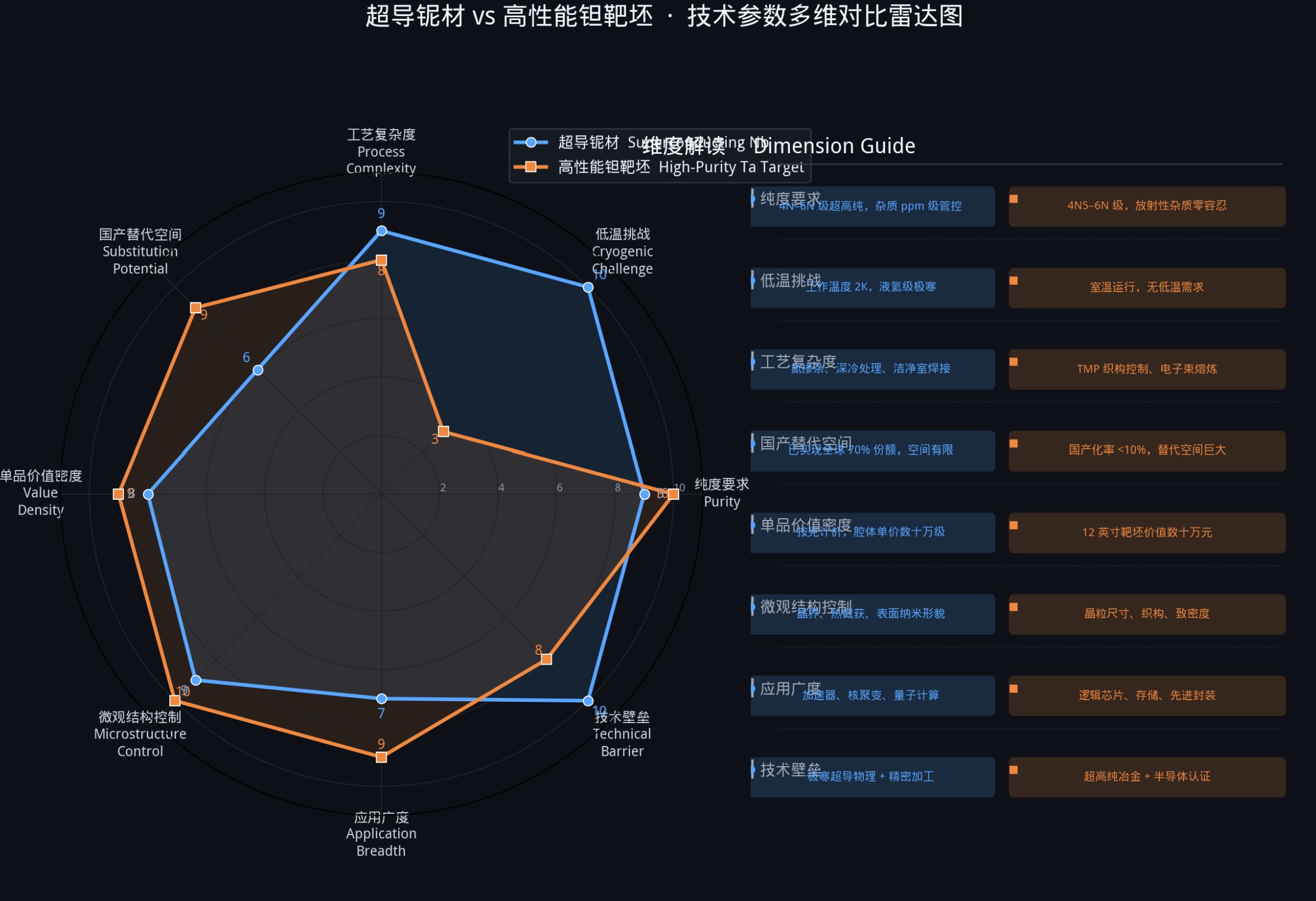
即便微量的杂质或微小的表面缺陷,都可能成为“热点”(Quench),破坏超导态。因此,用于制造超导腔的铌材必须具备极高的化学纯度(通常达到4N-5N,即99.99%-99.999%),且经过复杂的表面处理工艺,去除微米级的瑕疵。这种对完美的极致追求,使得高性能铌材的生产成为一门融合了冶金学、低温物理和精密加工的尖端艺术。
Even trace impurities or minute surface defects can act as "hotspots" (quenches), disrupting the superconducting state. Consequently, niobium used for fabricating superconducting cavities must possess exceptional chemical purity (typically 4N-5N, or 99.99%-99.999%) and undergo complex surface treatments to eliminate micrometer-scale flaws. This relentless pursuit of perfection elevates the production of high-performance niobium into a sophisticated art form, blending metallurgy, cryogenic physics, and precision machining.
1.3 应用前沿:照亮微观宇宙的灯塔
1.3 Frontiers of Application: Beacons Illuminating the Micro-Cosmos
超导铌材的应用,大多与人类的终极科学问题相连。
Applications of superconducting niobium are largely intertwined with humanity's ultimate scientific inquiries.
-
大型粒子加速器(如LHC): 位于欧洲核子研究中心(CERN)的大型强子对撞机(LHC),其核心加速部件便是由数千个铌制四极腔组成。正是这些“冷冰冰”的金属,让科学家得以捕捉到“上帝粒子”——希格斯玻色子的踪迹。
-
Large Particle Accelerators (e.g., LHC): The Large Hadron Collider (LHC) at CERN relies on thousands of niobium four-pole cavities as its core accelerating components. It is these "cold" metals that enabled scientists to detect traces of the "God Particle"—the Higgs boson.
-
自由电子激光(XFEL): 这是目前最亮的X射线光源,能够拍摄分子尺度的电影。其长达数公里的加速器隧道中,布满了高精度的铌超导腔。
-
X-ray Free-Electron Lasers (XFEL): Representing the brightest X-ray sources available, XFELs can capture "movies" at the molecular scale. Their multi-kilometer-long accelerator tunnels are lined with high-precision niobium superconducting cavities.
-
核聚变能源: 在托卡马克装置中,超导铌钛或铌三锡材料用于制造约束高温等离子体的强大磁体,是人类实现可控核聚变的基石。
-
Nuclear Fusion Energy: In tokamak devices, superconducting niobium-titanium or niobium-tin alloys are utilized to construct powerful magnets for confining high-temperature plasma—a cornerstone for achieving controlled nuclear fusion.
随着深空探测和低频射电天文学的发展,超导铌材也在高灵敏度探测器中扮演着关键角色,帮助人类倾听宇宙诞生之初的“余音”。
With advancements in deep-space exploration and low-frequency radio astronomy, superconducting niobium also plays a pivotal role in highly sensitive detectors, aiding humanity in listening to the "afterglow" of the universe's birth.

第二章:原子之雨——高性能钽靶坯的精密制造
Chapter 2: Rain of Atoms — Precision Manufacturing with High-Performance Tantalum Sputtering Targets
2.1 物理气相沉积(PVD):芯片的“镀金”时代
2.1 Physical Vapor Deposition (PVD): The "Gilded" Era of Chips
如果说超导铌材服务于宏观的大科学装置,那么钽(Tantalum)则深耕于微观的集成电路世界。
While superconducting niobium serves macroscopic mega-science facilities, tantalum delves deep into the microscopic realm of integrated circuits.
在现代半导体制造中,物理气相沉积(PVD)是一项核心技术。想象一下,在一个高真空的环境中,通过高能离子轰击一块固体源材料——这就是“靶材”(Target)。靶材表面的原子被撞击出来,像雨滴一样均匀地洒落在下方的硅晶圆(Wafer)表面,形成一层纳米级的薄膜。
In modern semiconductor manufacturing, Physical Vapor Deposition (PVD) is a core technology. Imagine a solid source material—the "target"—placed in a high-vacuum environment. High-energy ions bombard this target, dislodging atoms from its surface. These atoms then "rain down" uniformly onto the silicon wafer below, forming a nanometer-thin film.
高性能钽靶坯,正是这场“原子之雨”的源头。
High-performance tantalum sputtering targets are precisely the source of this "rain of atoms."
2.2 为何是钽?阻挡层的艺术
2.2 Why Tantalum? The Art of the Diffusion Barrier
随着芯片制程进入纳米节点(如28nm及以下),晶体管之间的连线(Interconnects)变得越来越细。为了防止铜原子(用于连线的主要金属,导电性好但极易扩散)钻进周围的绝缘层(二氧化硅)造成短路,工程师必须在铜和绝缘层之间铺设一层“铜扩散阻挡层”。
As chip fabrication nodes shrink into the nanoscale (e.g., 28nm and below), interconnects between transistors become increasingly fine. To prevent copper atoms—the primary metal used for interconnects due to its excellent conductivity but high diffusivity—from migrating into the surrounding insulating layer (silicon dioxide) and causing short circuits, engineers must insert a "copper diffusion barrier" between them.
钽,因其卓越的化学稳定性、耐高温性以及与铜和绝缘介质良好的粘附性,成为了这一角色的最佳人选。此外,钽也被用于制造高容量电容器的阳极,广泛应用于手机、电脑等电子产品中。
Tantalum, owing to its outstanding chemical stability, high-temperature resistance, and excellent adhesion to both copper and dielectric insulators, is the ideal candidate for this role. Additionally, tantalum serves as the anode material in high-capacity capacitors, widely deployed in consumer electronics such as smartphones and computers.
2.3 靶坯的极致要求:均匀与致密
2.3 Extreme Demands on Targets: Uniformity and Density
高性能钽靶坯并非简单的金属块,它的制造难度极高:
High-performance tantalum sputtering targets are far from mere metal blocks; their fabrication is exceedingly challenging:
-
超高纯度(Ultra-High Purity): 半导体级钽靶的纯度通常要求在 4N5 (99.995%) 到 6N (99.9999%) 之间。任何微量的碱金属(如钠、钾)或放射性元素(如铀、钍)都会污染晶圆,导致芯片失效。这就要求从钽矿提纯开始,每一步都要严格控制。
-
晶粒均匀性(Grain Uniformity): 靶材的晶粒大小直接影响溅射速率和薄膜的均匀性。如果晶粒大小不一,溅射出来的原子流就会忽大忽小,导致芯片表面膜厚不均。因此,必须通过复杂的冶金工艺(如热机械处理)精确控制晶粒尺寸在狭窄的范围内。
-
高致密性(High Density): 靶材必须接近理论密度,不能有气孔。否则,在真空溅射过程中,气孔内的气体释放会导致“微弧放电”,在芯片表面留下难以修复的缺陷(Particle)。
-
织构控制(Texture Control): 先进的靶材还需要控制晶面的择优取向(Texture),以优化溅射原子的角分布,确保覆盖复杂的三维结构(如高深宽比的沟槽)。
-
Ultra-High Purity: Semiconductor-grade tantalum targets typically require purities ranging from 4N5 (99.995%) to 6N (99.9999%). Trace amounts of alkali metals (e.g., sodium, potassium) or radioactive elements (e.g., uranium, thorium) can contaminate wafers, rendering chips defective. This necessitates stringent control throughout the entire process, starting from tantalum ore refining.
-
Grain Uniformity: The grain size of the target directly impacts the sputtering rate and the uniformity of the deposited film. Non-uniform grain sizes lead to fluctuating atomic fluxes, resulting in uneven film thickness across the wafer. Hence, sophisticated metallurgical processes (e.g., thermomechanical treatments) are required to tightly control grain dimensions.
-
High Density: Targets must approach theoretical density and be free of pores. Otherwise, gas trapped in pores could release during vacuum sputtering, causing "micro-arcing" and leaving irreparable defects (particles) on the chip surface.
-
Texture Control: Advanced targets also require control over crystallographic texture (preferred orientation) to optimize the angular distribution of sputtered atoms, ensuring conformal coverage over complex 3D structures (e.g., high-aspect-ratio trenches).
2.4 应用前沿:从AI芯片到先进封装
2.4 Frontiers of Application: From AI Chips to Advanced Packaging
随着人工智能(AI)和大数据时代的到来,芯片的运算速度呈指数级增长,这对互连技术提出了更高要求。
With the advent of the AI and Big Data era, computational speeds are increasing exponentially, placing higher demands on interconnect technologies.
-
先进制程(Sub-10nm): 在极小的工艺节点下,钽阻挡层必须做得极薄(几个原子层厚)且连续无针孔。这推动了钽靶材向更高纯度和更精细微观结构发展。
-
Advanced Nodes (Sub-10nm): At extremely small nodes, tantalum barrier layers must be ultra-thin (mere angstroms thick) yet continuous and pinhole-free. This drives the development of tantalum targets towards even higher purity and finer microstructures.
-
2.5D/3D封装与HBM: 高带宽内存(HBM)等先进封装技术需要填充极深的硅通孔(TSV)。钽作为种子层和阻挡层,必须能够完美覆盖这些深孔的侧壁,这对靶材溅射的保形性(Conformality)提出了严苛挑战。
-
2.5D/3D Packaging & HBM: Advanced packaging technologies like High Bandwidth Memory (HBM) require filling extremely deep Through-Silicon Vias (TSVs). Tantalum, serving as both seed layer and barrier, must perfectly conform to the sidewalls of these deep vias, posing severe challenges to the conformality of sputter deposition.
第三章:殊途同归的材料哲学
Chapter 3: A Shared Material Philosophy Despite Divergent Paths
虽然超导铌材和高性能钽靶坯一个服务于极寒的真空,一个服务于半导体的真空,但它们的底层逻辑惊人地相似。
Although superconducting niobium operates in the frigid vacuum of particle accelerators while high-performance tantalum targets function in the vacuum of semiconductor fabs, their underlying logic reveals striking similarities.
3.1 纯度即性能
3.1 Purity Equals Performance
无论是铌材中的氧含量,还是钽材中的杂质总量,都直接决定了最终产品的成败。在这两个领域,“纯度”不再是化学概念,而是物理性能的代名词。 99.99%和99.999%的区别,往往意味着能否实现超导,或者能否造出良率的芯片。
Whether it concerns oxygen content in niobium or total impurity levels in tantalum, both directly dictate the success of the final product. In these domains, "purity" transcends mere chemistry; it is synonymous with physical performance. The difference between 99.99% and 99.999% often determines whether superconductivity can be achieved or if high-yield chips can be manufactured.
3.2 微观组织决定宏观命运
3.2 Microstructure Dictates Macro Fate
晶体结构、晶粒尺寸、晶界状态……这些微观特征,决定了铌材能否承受百兆伏特的电场,决定了钽原子能否均匀覆盖晶圆。现代高端金属材料科学的竞争,本质上是对微观世界操控能力的竞争。
Crystal structure, grain size, grain boundary characteristics... these microscopic features determine whether niobium can withstand electric fields of hundreds of megavolts per meter, or whether tantalum atoms can uniformly coat a wafer. Competition in modern advanced materials science is, at its core, a competition in the ability to manipulate the microscopic world.
3.3 国家战略资源
3.3 Strategic National Resources
铌和钽都是我国对外依存度较高的稀缺战略矿产资源。从原矿冶炼到高纯提纯,再到最终的精密加工,建立自主可控的全产业链,不仅是经济问题,更是国家安全与科技独立的基石。
Both niobium and tantalum are scarce strategic mineral resources with high import dependency in many nations. Establishing a self-reliant and controllable industrial chain—spanning from raw ore smelting and high-purity refining to final precision machining—is not merely an economic issue but a cornerstone of national security and technological sovereignty.
结语:看不见的基石
Conclusion: The Invisible Cornerstone
当我们惊叹于CERN发现新粒子的宏伟,或是感慨于智能手机芯片的算力飞跃时,请不要忘记那些隐藏在背后的材料英雄。
As we marvel at the grand discoveries of new particles at CERN or the leaps in computing power of smartphone chips, let us not forget the unsung heroes of materials science behind the scenes.
超导铌材,在极寒中无声地加速粒子,探索宇宙的真理;高性能钽靶坯,在真空室里播撒原子,构筑数字文明的基石。它们代表了人类对极致性能的不懈追求,也是现代工业皇冠上两颗低调而璀璨的宝石。
Superconducting niobium silently accelerates particles in extreme cold, probing the truths of the cosmos; high-performance tantalum sputtering targets scatter atoms within vacuum chambers, laying the foundation for our digital civilization. They embody humanity's relentless pursuit of ultimate performance and stand as two understated yet brilliant gems atop the crown of modern industry.
在未来,随着可控核聚变技术的突破和摩尔定律的延续,这两种材料必将在更广阔的舞台上,继续它们的微观征途。
Looking ahead, with breakthroughs in controlled nuclear fusion and the continued evolution of Moore's Law, these two materials are poised to continue their microscopic odyssey on an even grander stage.
词汇表 | Glossary
-
超导态 (Superconducting State): 材料在特定温度下电阻为零的状态。
-
迈斯纳效应 (Meissner Effect): 超导体排斥内部磁场的现象。
-
射频超导腔 (RF Superconducting Cavity): 利用超导材料制成的微波谐振腔,用于加速带电粒子。
-
溅射 (Sputtering): 利用离子轰击靶材,使表面原子逸出并沉积在基底上的物理过程。
-
铜扩散阻挡层 (Copper Diffusion Barrier): 防止铜原子扩散进入周围介质的隔离层。
-
高纯钽 (High-Purity Tantalum): 纯度在99.99%(4N)以上的金属钽,主要用于半导体和电子行业。
此文由 怡心湖 编辑,若您觉得有益,欢迎分享转发!:首页 > 常识论 » 极寒之舞与原子之雨:超导铌材与高性能钽靶坯的微观世界征途 Dance in the Cold, Rain of Atoms: The Microscopic Odyssey of Supercondu
 核聚变堆超导磁体应用